Development of custom electronic boards with CNC Router.
During this week, we also carried out teamwork through the ZOOM platform. To do this, we used a multimeter to perform power consumption tests on a device or load. In this case, we focused on measuring the consumption of energy of a minipump.
Main features
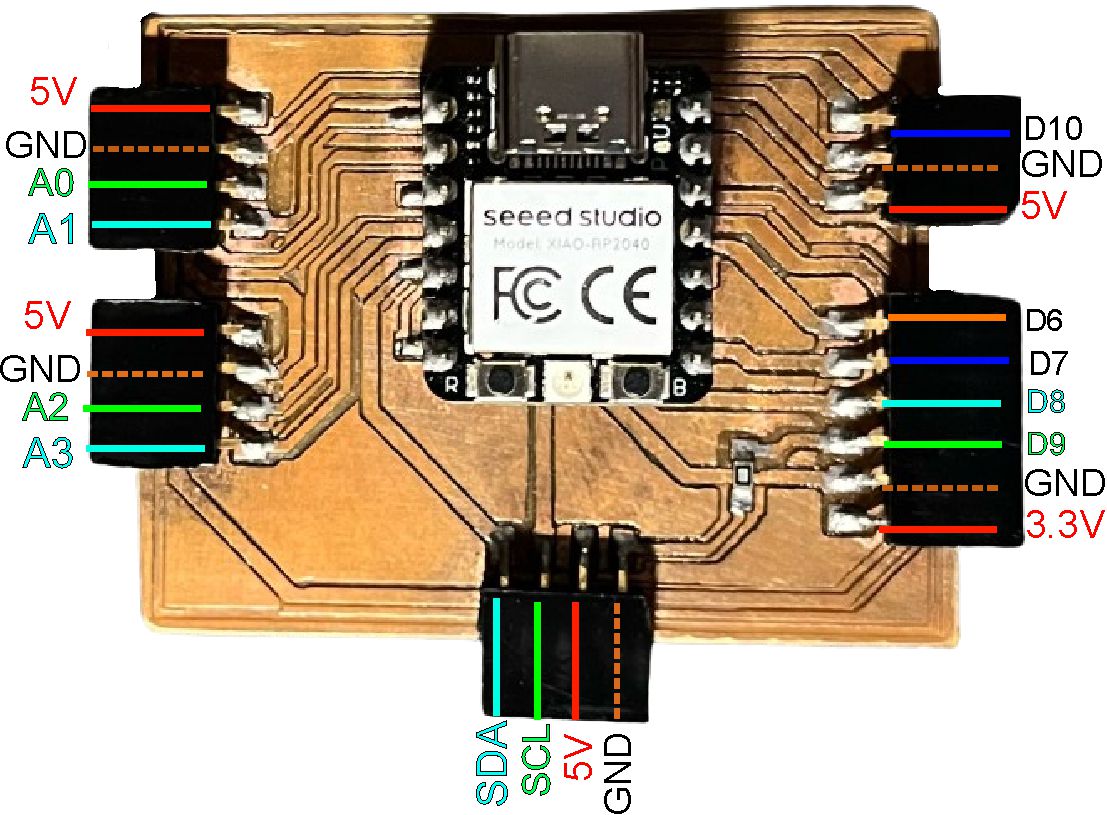
To carry out the power consumption tests, we use a multimeter, a mini pump model JT-180B, a constructed output board, the XIOA RP2040 and a 6V battery with a capacity of 4A.
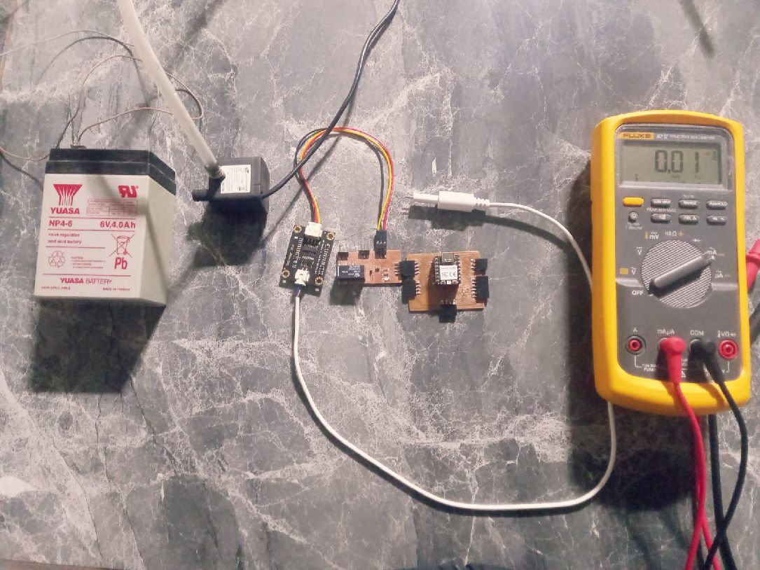
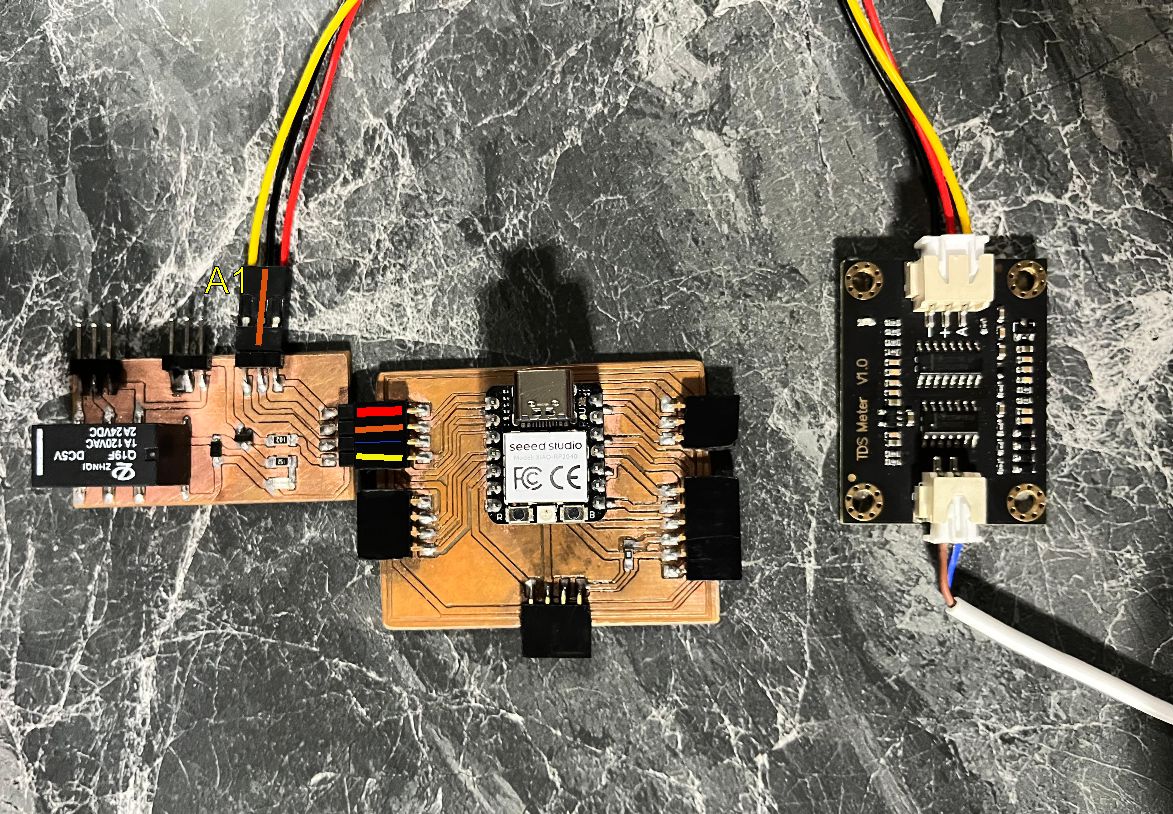
The first step is to place the components on the motherboard: the controller or board with the relay, the TDS sensor and the battery.
It is also important to position the multimeter correctly, with the black lead in the COM position and the red lead in the mA position.
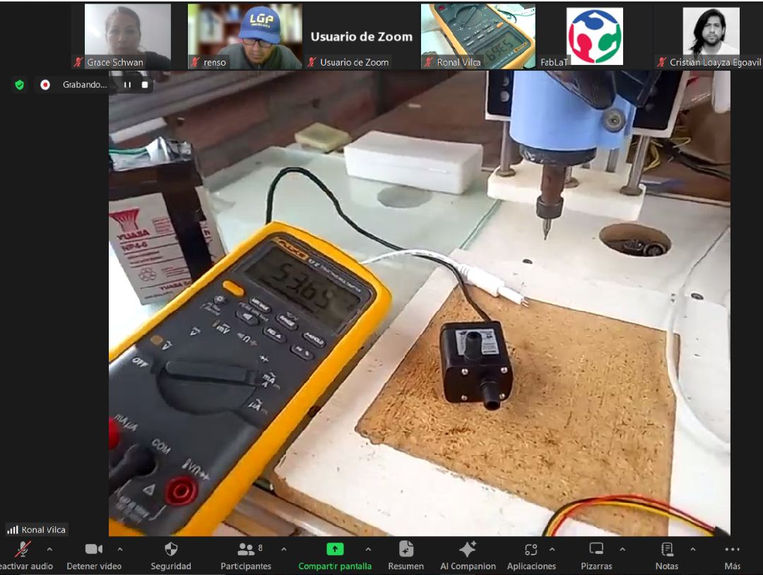
When carrying out the measurements, it can be seen that the energy consumption of this minipump is 53.95 mA. This information is crucial to understand the energy requirement of the pump and ensure adequate power in the circuit design.
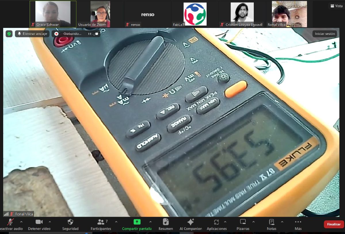
During our experience this week with the multimeter, we understood its vital importance in the electronic field. This device allows us to measure and confirm key values of electronic components, such as resistance, perform diode tests, evaluate the continuity of circuits and, fundamentally, determine the energy consumption of our loads, as in the case of the minipump. This information is crucial to selecting a suitable battery and correctly sizing the electronic components needed for our project.
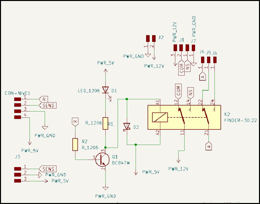
For individual work, a board was designed using KiCad software with the objective of controlling a minipump, which is an actuator that demands more than a simple resistance in the circuit. In this case, a relay was incorporated that, when activated, will allow the load to be activated by opening the corresponding step.
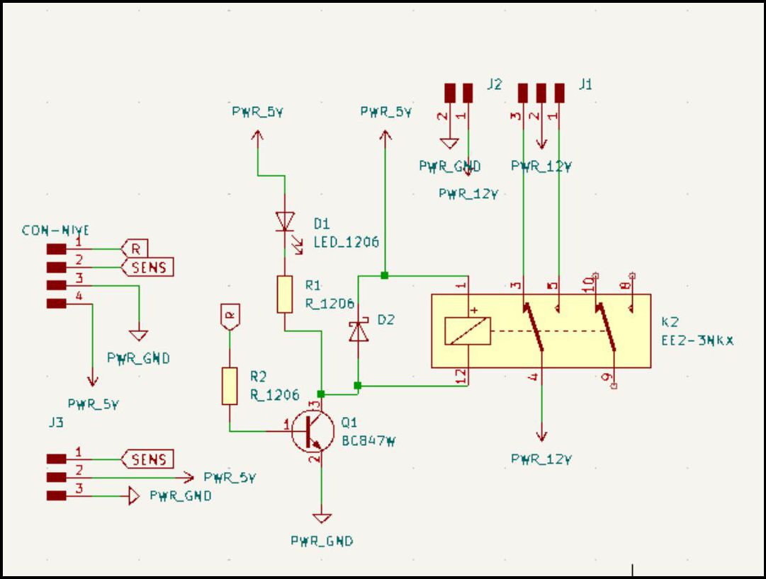
The components needed for this board include a relay, resistors, an indicator LED, a transistor that will amplify the current and activate the relay, as well as their respective header connectors.
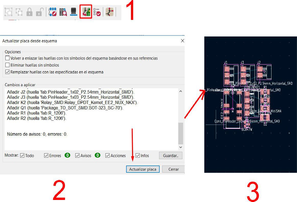
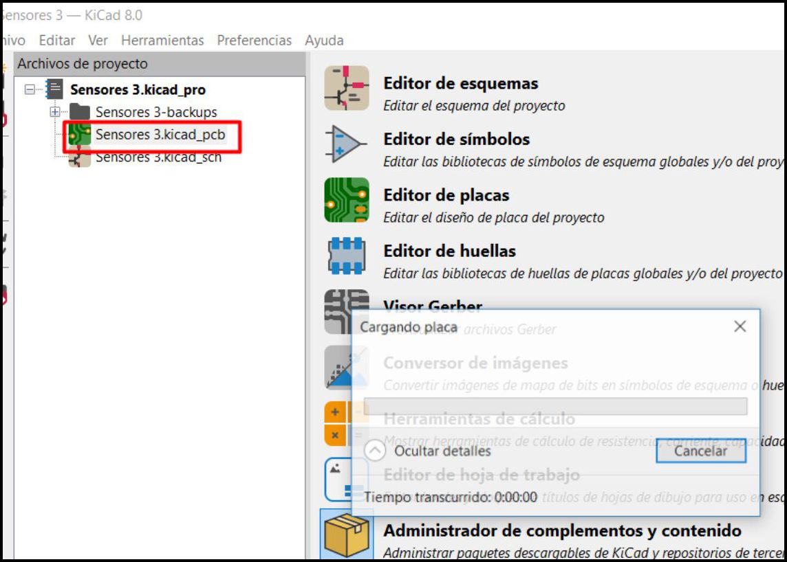
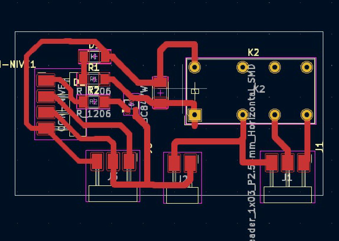
After completing the schematic, the next step is to move to the PCB design. In this stage, the packages or symbols that represent the actual size components are imported. This is done by simply updating the component library in the toolbar, as indicated in the images.
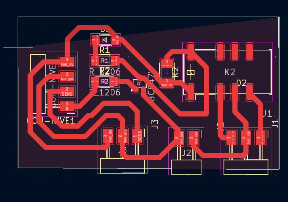
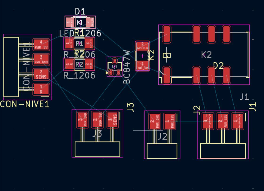
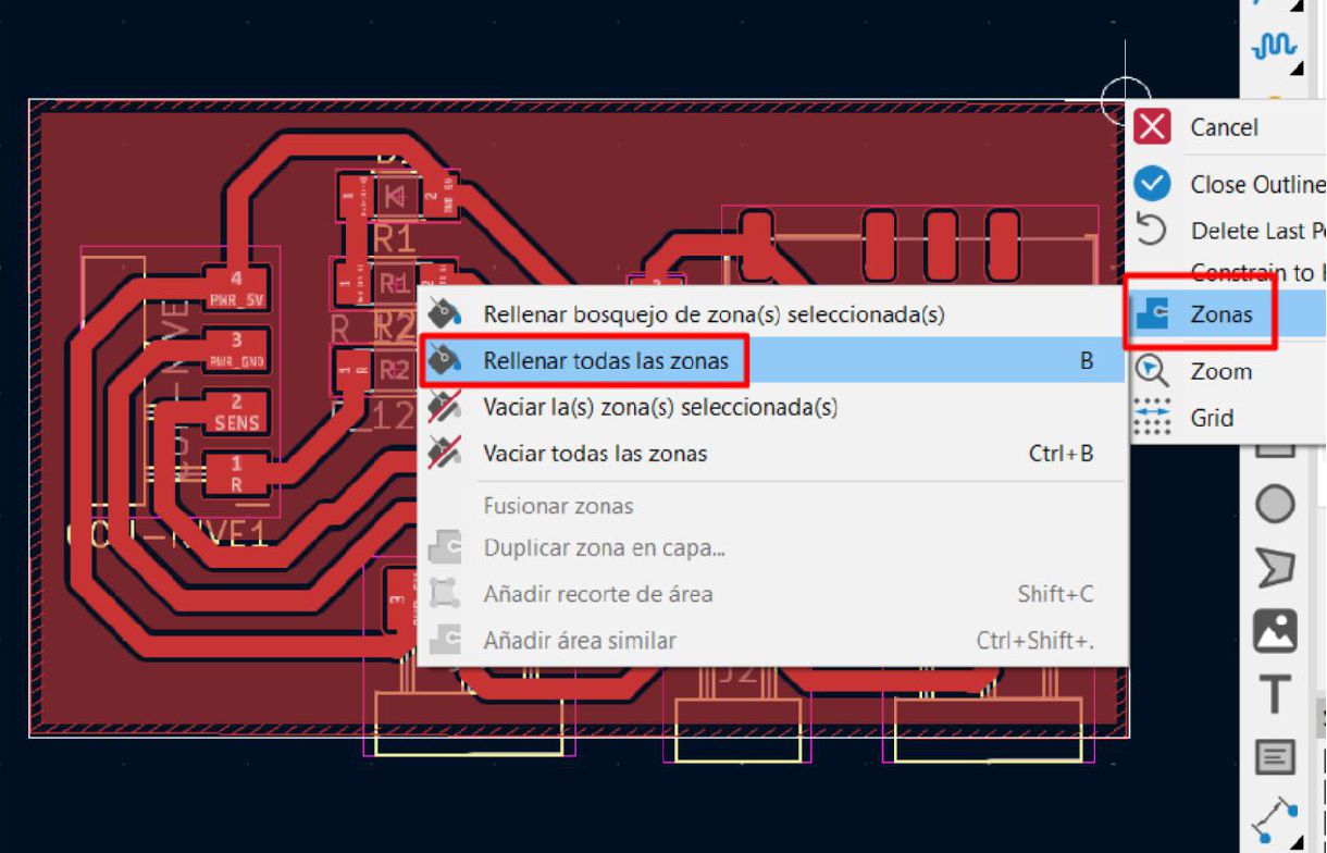
In this step, we proceed to distribute the components as necessary on the printed circuit board (PCB) and perform routing, which consists of tracing the electrical connections between each component.
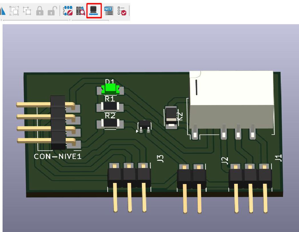
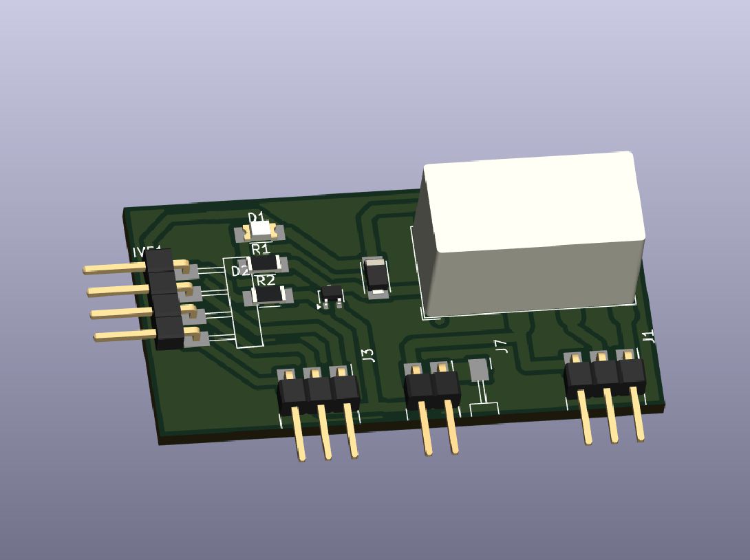
As you can see, the board is ready and you can visualize in 3D what it will look like once all the components are soldered in place.
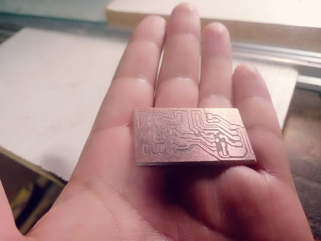
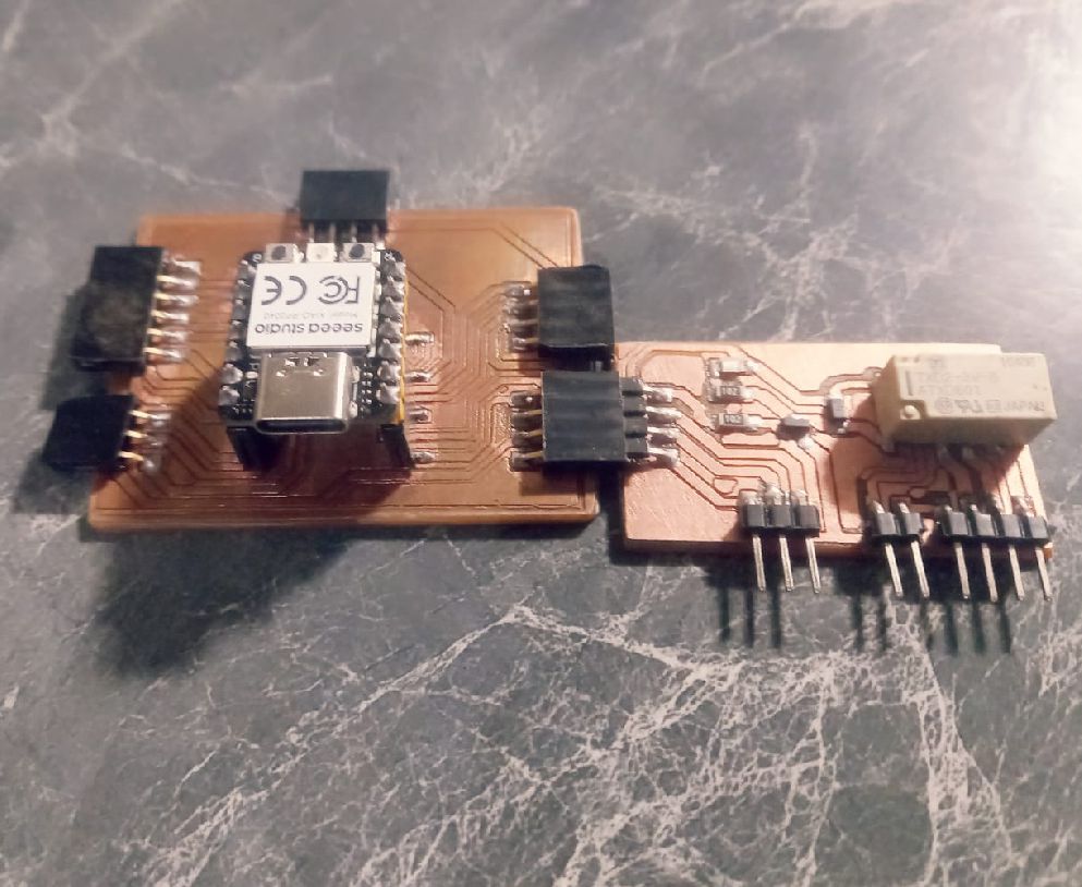
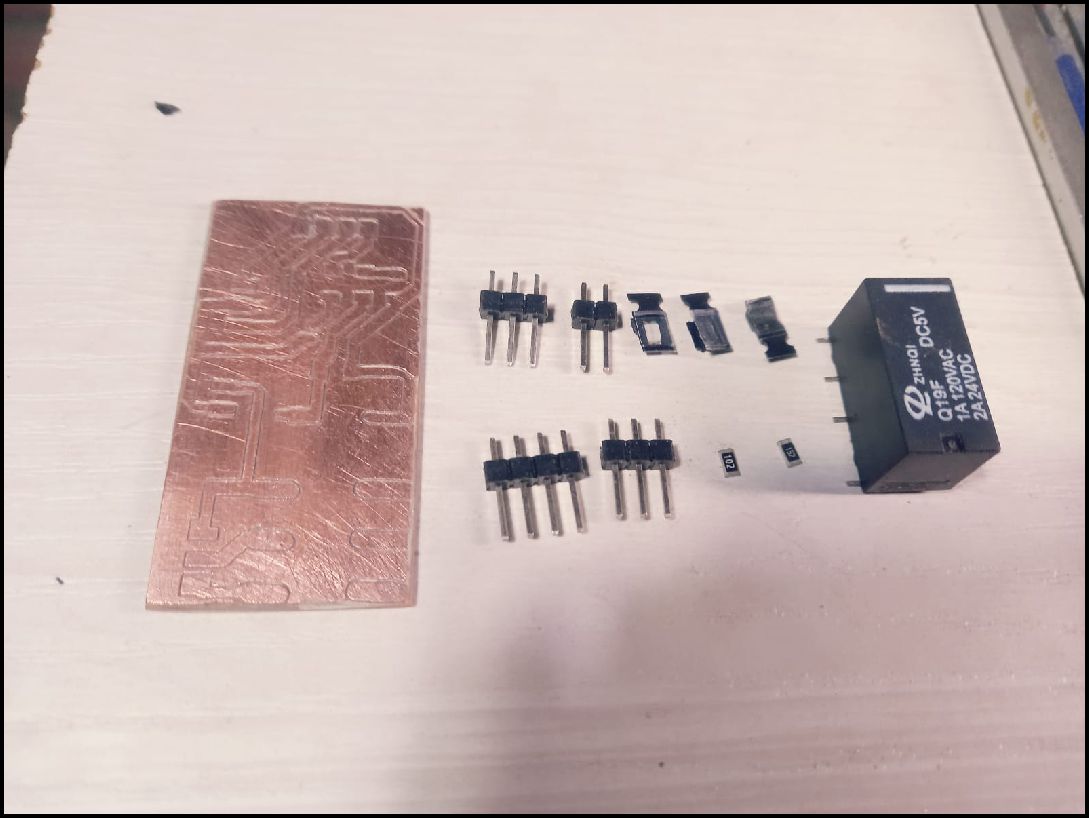
With the board already developed on the CNC, the next step is to solder the electronic components in place.
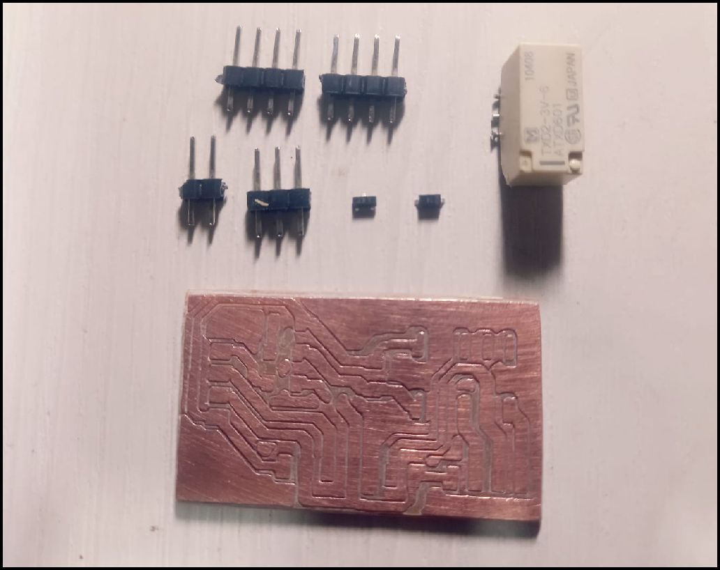
We begin by soldering the relay and the diode, while we review the specifications of each component in detail.
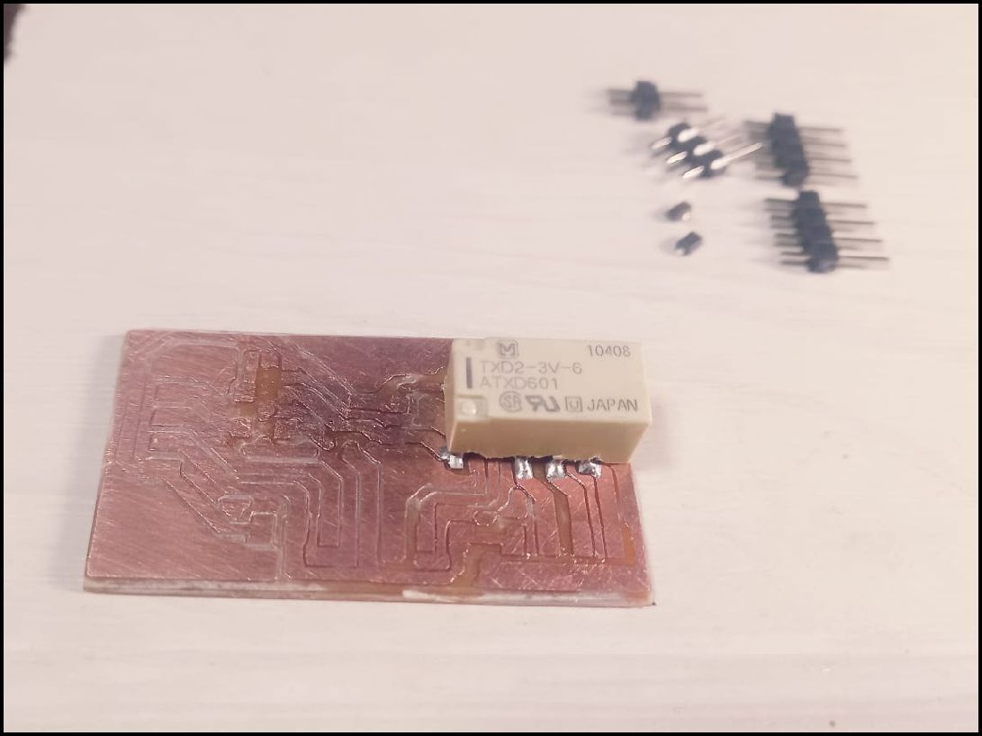
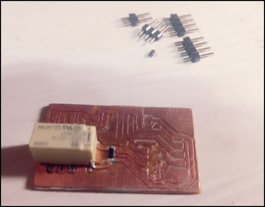
After soldering the relay and diode, we continue with the 1.5k resistor that is connected in series with the LED diode. Next, we solder the 1k resistor that goes to the base of the J3Y transistor, followed by the headers as shown in the images.
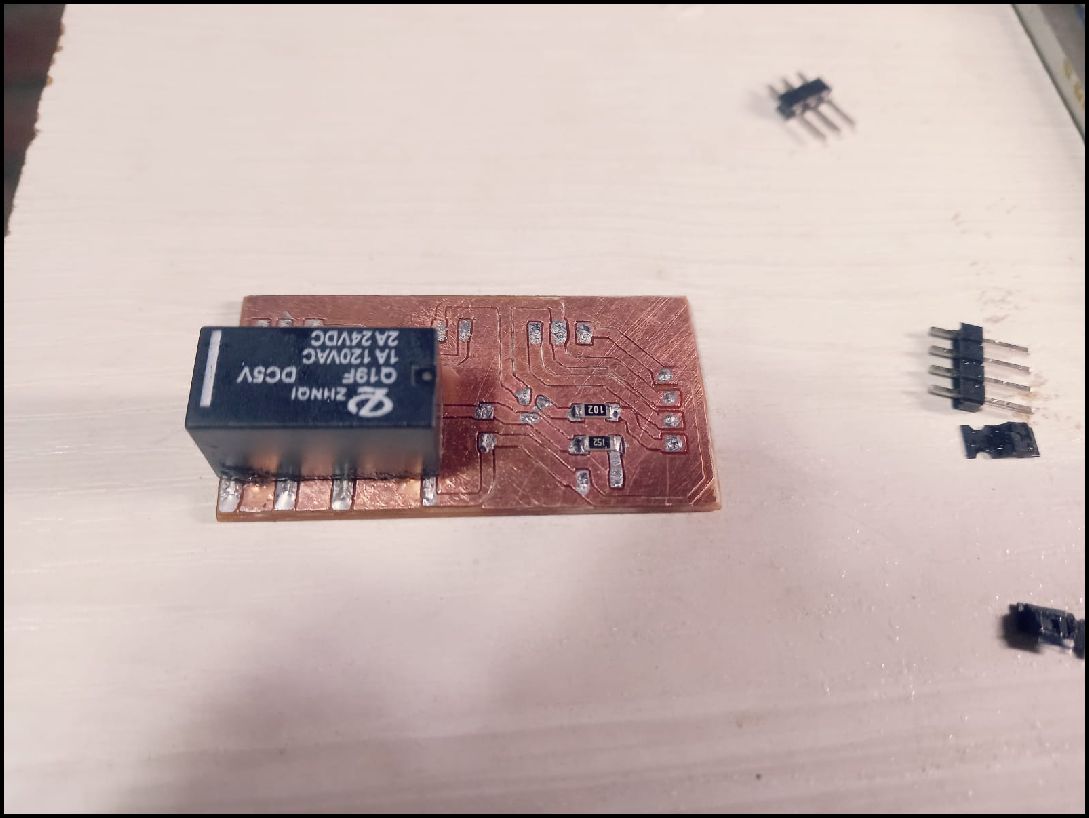
Finally, all the remaining components are connected and how they will be interconnected on the motherboard is presented.
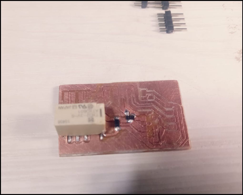
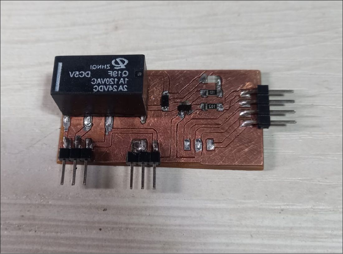
We found a problem after soldering the parts and performing a test; Unfortunately, the system was not working. I performed measurements on all components, including diodes, resistors, and transistors, and they were all within normal values. However, when measuring the relay, I discovered the source of the error. The coil was intact, but the contact on the NC (normally closed) side did not open, while the contact on the NO (normally open) side remained active, which explained the system's non-function.

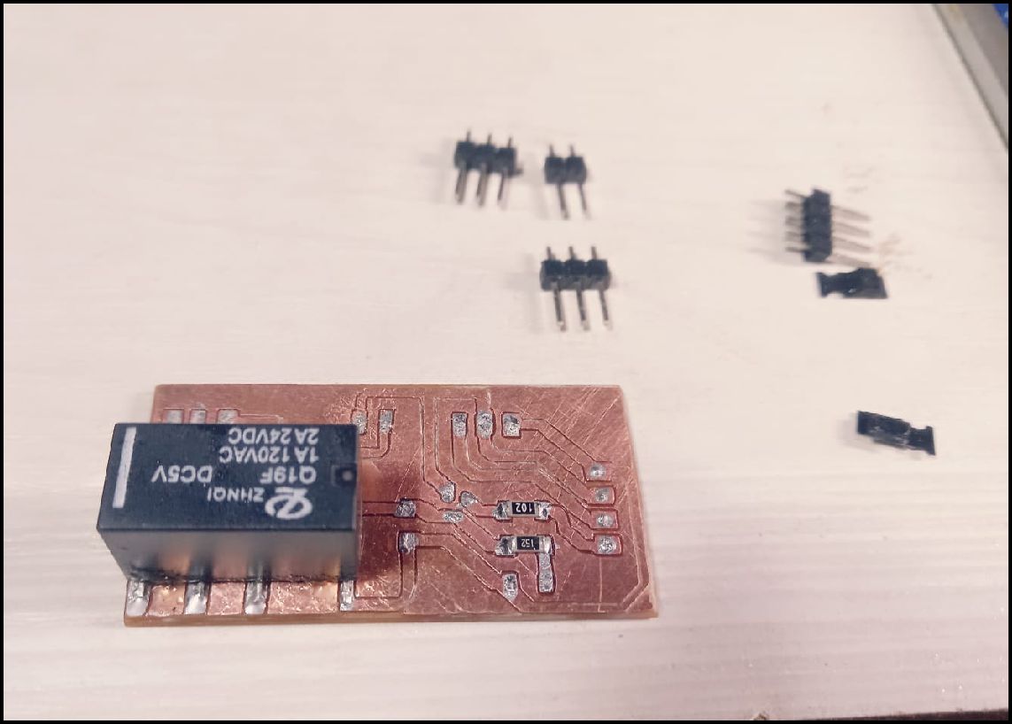
I made a mistake by not taking measurements before soldering the components, and even before designing the entire board taking into account the dimensions of the relay, since it was the only one I had available. Now, it is time to rectify the situation and change the component in the design for a new relay, also considering its dimensions, since I do not have the SMD type
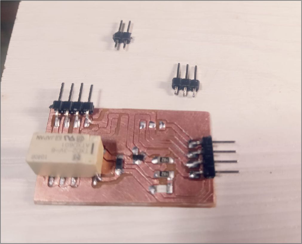
Every mistake represents a valuable learning opportunity that stays with us. In my case, I will choose to replace the relay with a new board that will use a DIP type mini relay, and the other components will follow the same specification.
Since all components are identical, with the only variation being the relay and board size, we will not face additional difficulties in the design phase.
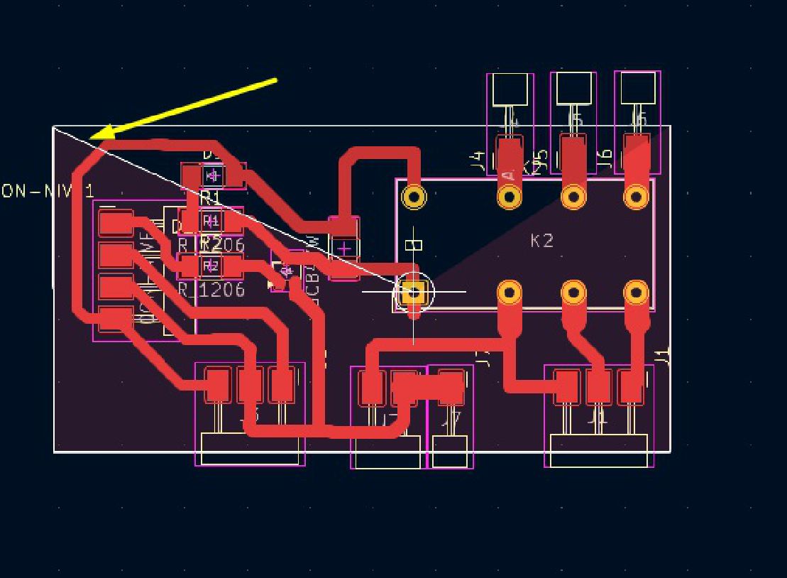
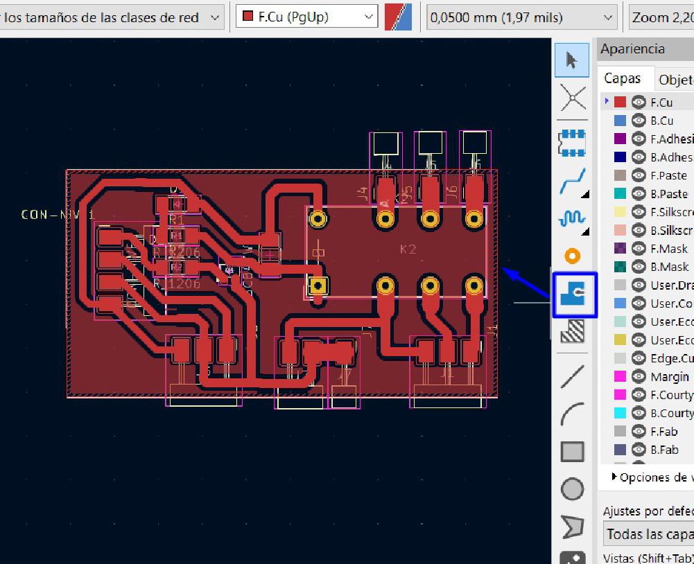
As you can see, the component change has been made. In this case, the footprint is wider, resulting in a larger plate working area. The procedure remains the same; The component that has been modified is simply routed, as shown in the following image.
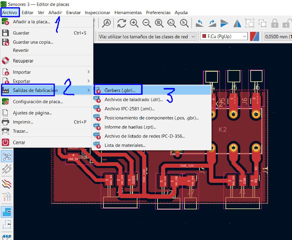
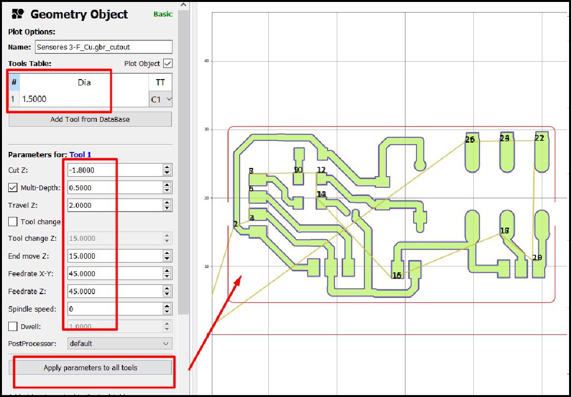
The following image shows the steps to follow to export Gerber files. These will be processed with the FlatCAM software and then machined with the CNC.
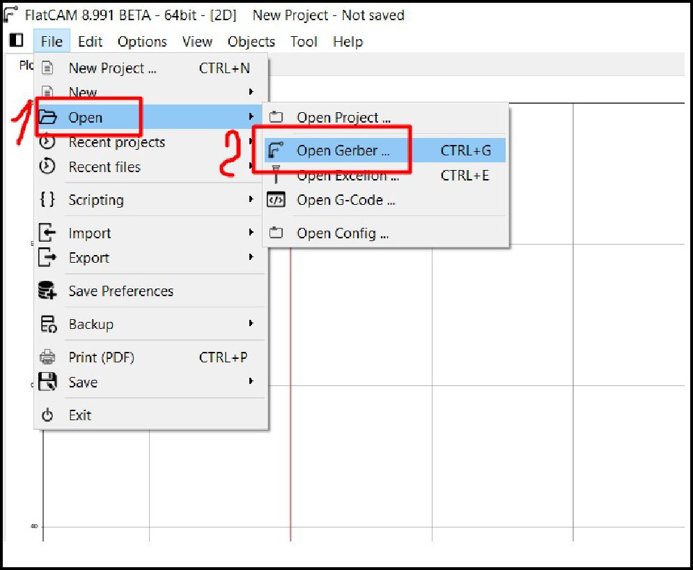
With the FlatCAM software already installed, the Gerber file previously exported from KiCad is imported to process it with a homemade CNC router.
The next step in the CNC machining process is to import the Gerber file into the Flatcam software and configure the corresponding parameters, such as the tool size, which in this case is 3.175 mm, and the tilt angle ranging from 0.1 up to 30 degrees.
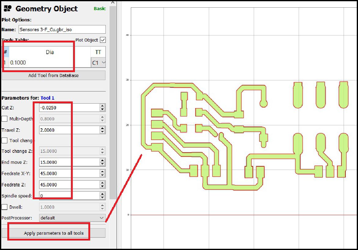
The next step involves setting up the roughing using the tool, setting a value of -0.0250 and the movements on the XYZ axes to 45 degrees. Once configured, the generated area will be displayed in blue. To finish, we simply click on "Generate
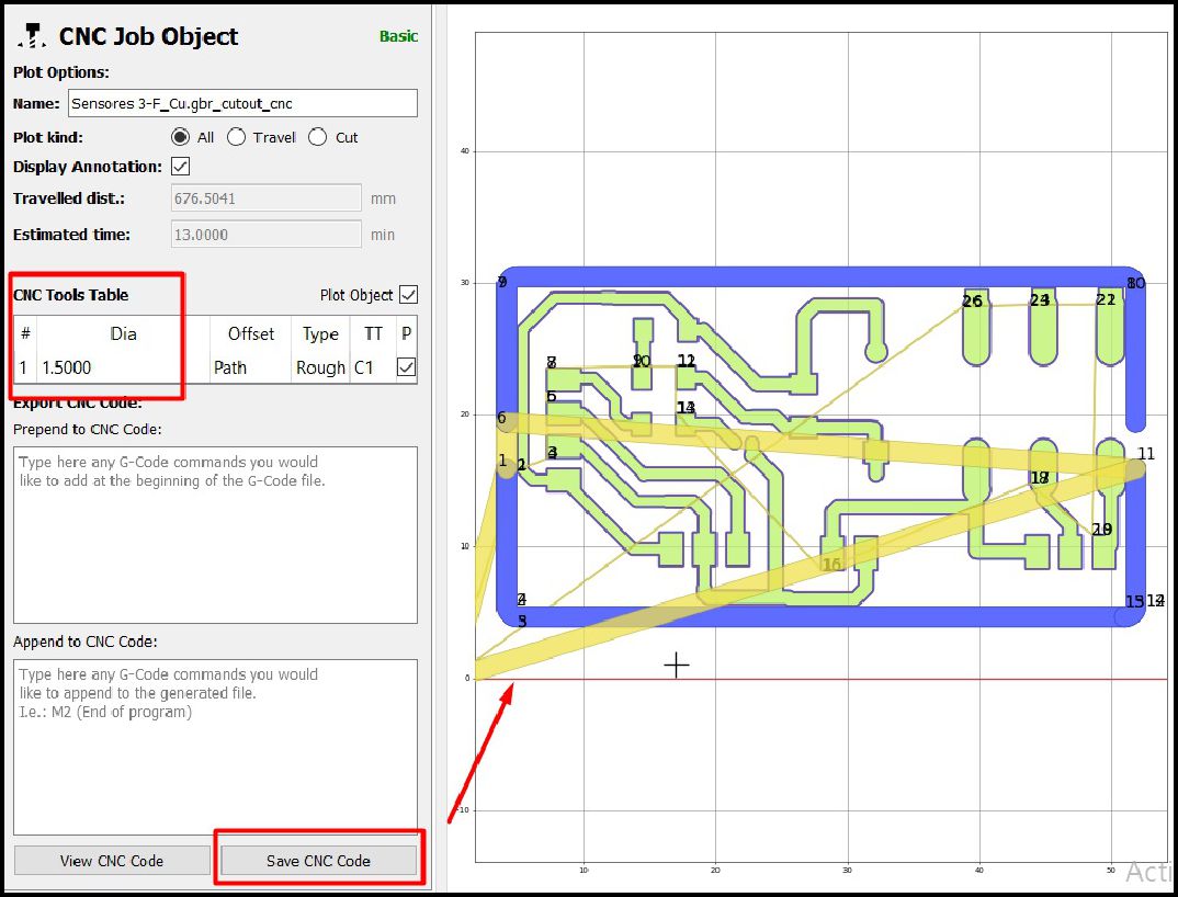
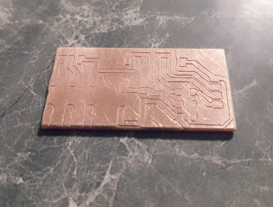
The following image shows how the plate looked after being processed with the CNC. This work was carried out in a single pass, at a depth of 0.025 mm below the Z axis.
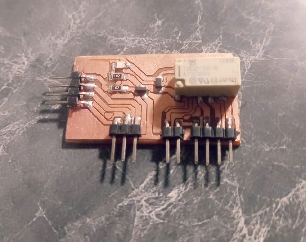
Once we have generated the G-code files, we proceed to the machining stage to obtain the desired plate. Once the board is obtained, we are ready to solder the electronic components in place.
The next step involves soldering the components, such as relays and resistors, following their arrangement on the board according to the previously established design.
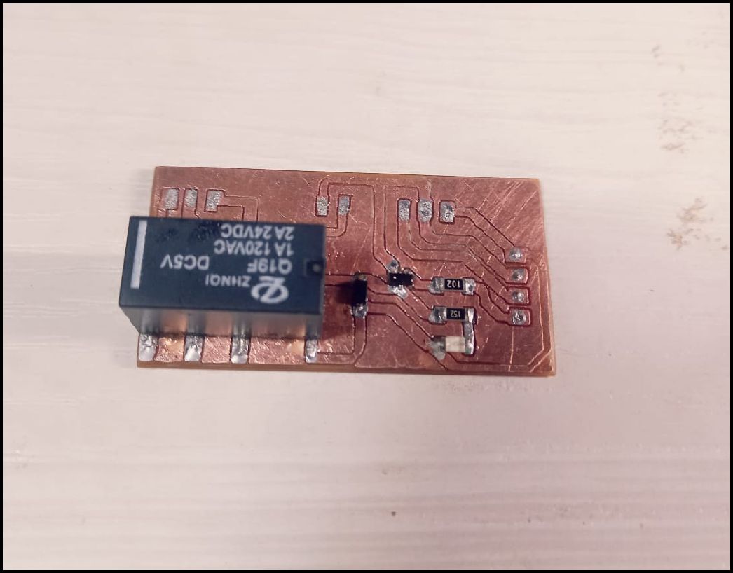
Yes, you can solder the components together on the board. This includes the J3Y transistor, LED, resistor and headers as necessary. It is important to follow the design and planned layout on the board to ensure correct connection and operation of the circuit.
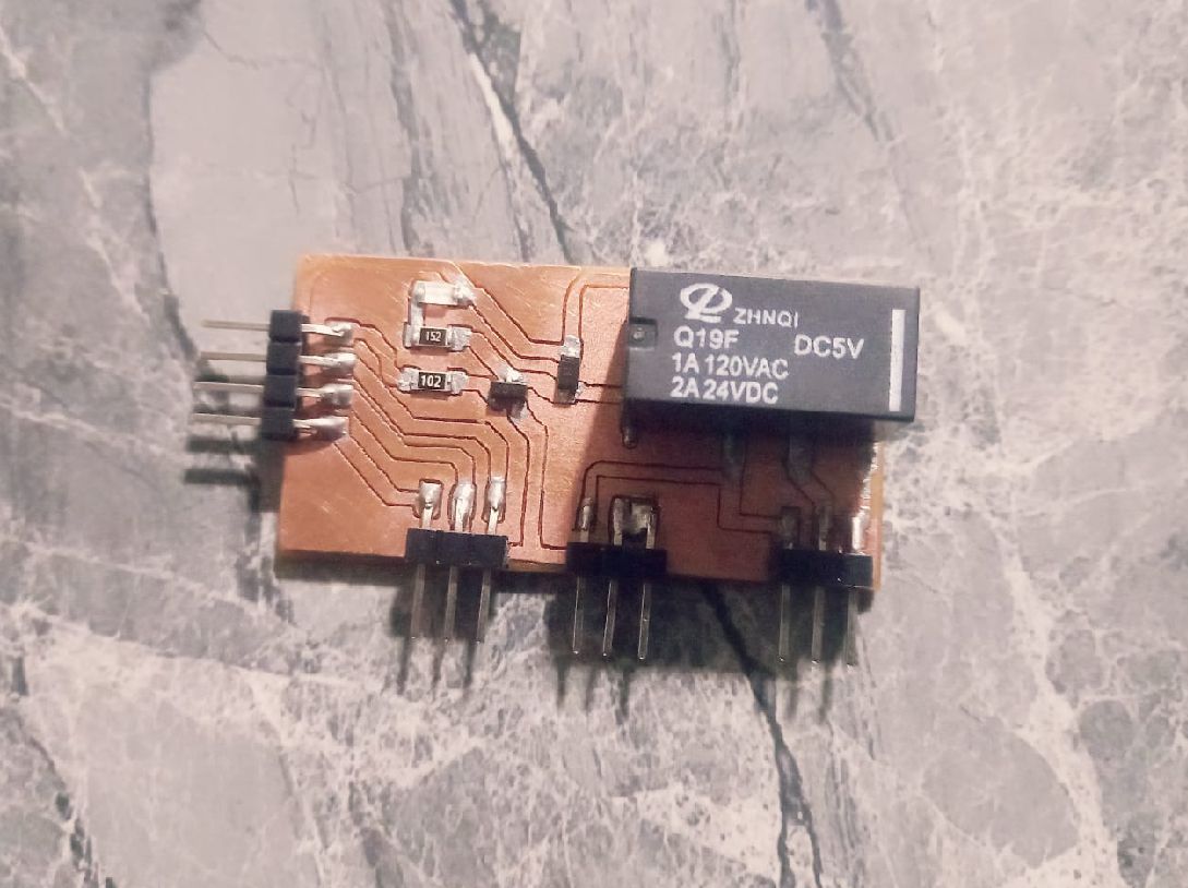
It was hard work, but we finally managed to complete a new board. This experience taught me an important lesson: always perform measurements of all components before starting the design of the electronic board. This prior approach allows us to avoid costly errors and ensure a more efficient manufacturing process.
1. schematic.kicad-sch
2. schematic.kicad-pcb
3. schematic.kicad-gbr
4. Pump-tds.ino
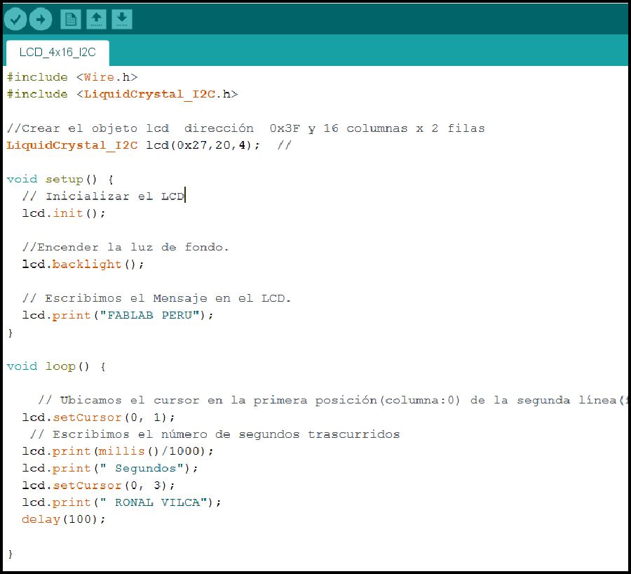
5. LCD_4x16_I2C.ino
Development of custom electronic boards with CNC Router.

Development of personalized keychains and ornaments with CNC Laser.
Development of custom machines "Desktop CNC Laser.

Huánuco is a Peruvian city, capital of the district, province and department of the same name in the north-central area of the country. The city has a population of 235,529 inhabitants. .